NEG's Glass Substrates for Next-Generation Semiconductors
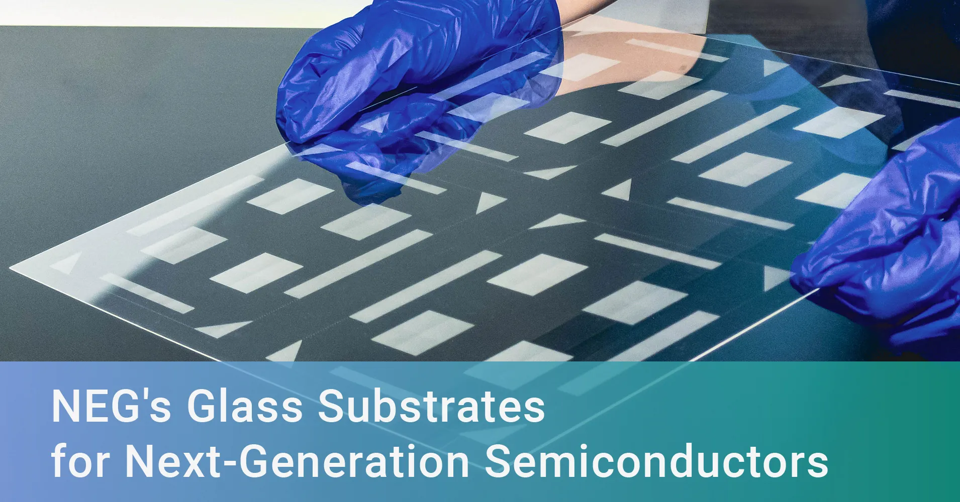
Glass is gaining attention as the next-generation semiconductor package substrates.
In recent years, the spread of generative AI and the advancement of autonomous driving have increased the demand for even higher-performance semiconductors. At the same time, the sharp increase in manufacturing costs has become an issue that cannot be ignored.
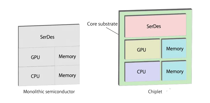
One solution to this problem is chiplets. Chiplets are a technology that enhances performance by integrating multiple chips into a single semiconductor package. However, this trend leads to larger interposers and package substrates, along with increasingly dense interconnects between chips.
Conventional resin-based package substrates have faced material limitations that made scaling up and increasing density difficult. Glass substrates are now gaining attention as the next-generation semiconductor package substrate.
To address these circumstances, Nippon Electric Glass (NEG) developed the glass-ceramic core substrate GC Core® and glass core substrates.
This article clearly explains how the glass substrates developed by NEG solve challenges in the scaling up and increasing density of semiconductor packages.
- • The Background Behind the Re-evaluation of Materials for Semiconductor Package Substrates
- • What Is a Glass Core Substrate?
- • Challenges with Glass Substrates
- • Features of NEG's Glass Substrates
- • Accelerating Development through Collaboration with Via Mechanics
- • Also Compatible with Laser Modification and Etching Methods
- • Summary: Strengths of NEG
The Background Behind the Re-evaluation of Materials for Semiconductor Package Substrates
One reason glass is gaining attention as a material for semiconductor package substrates is the proliferation of chiplet technology and the challenges facing resin substrates.
With the spread of chiplets, semiconductor package substrates are becoming larger and more densely packed.
A chiplet is an implementation technique that involves preparing multiple small chips specialized for specific functions instead of creating a single large semiconductor chip, then integrating them into a single semiconductor package.
Chiplets offer the following benefits:
• Cost reduction through yield improvement
• Easy to extend functionality
• Chips from different manufacturers can be combined
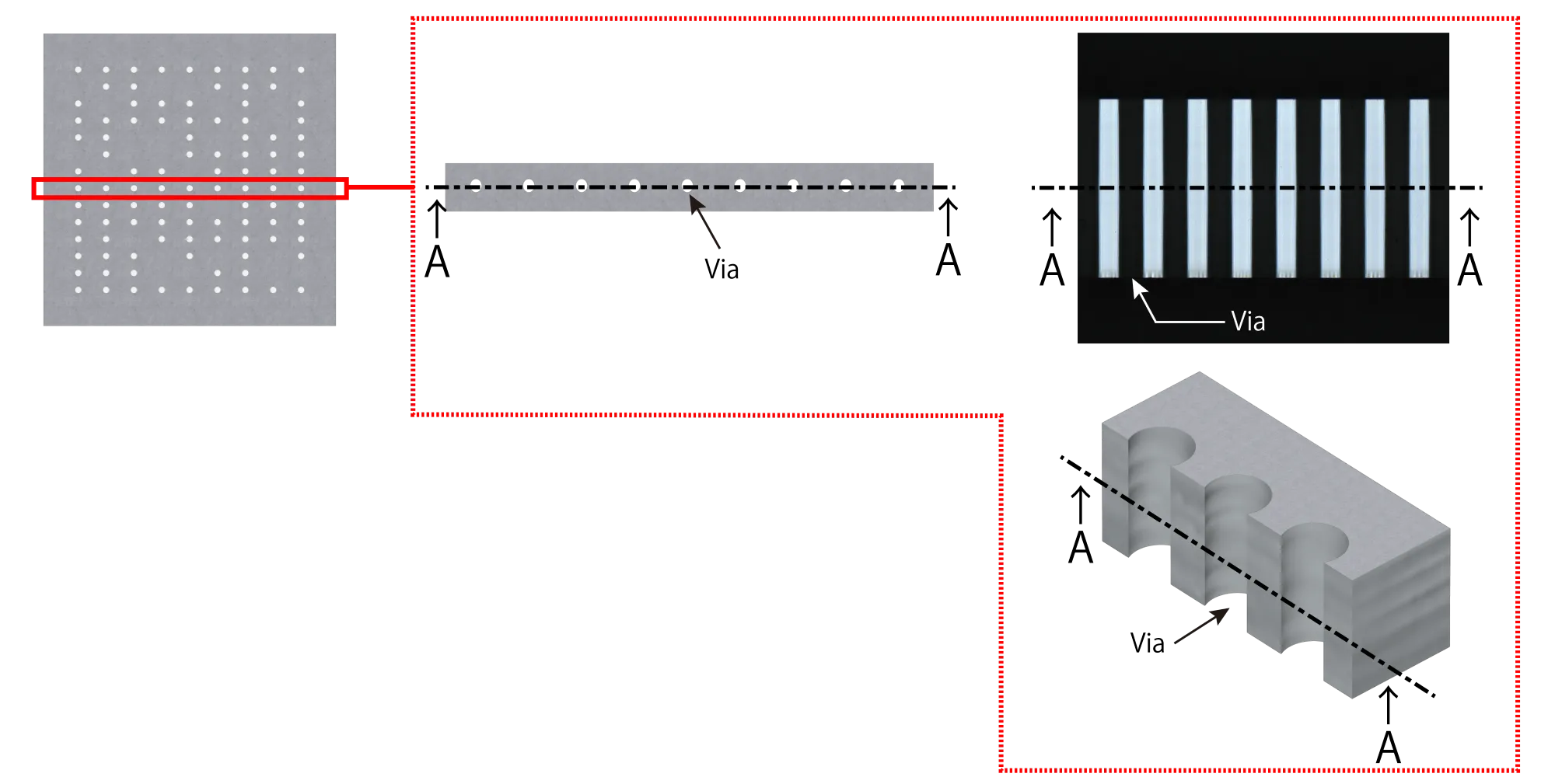
However, since chiplets mount multiple chips within a single semiconductor package, the core substrate forming the package's foundation tends to increase in size. Simultaneously, it is necessary to densely form fine interconnects between chiplets and numerous vias*1 on the core substrate, making high-precision processing technology indispensable.
-
1: A via is a hole provided in a semiconductor substrate to electrically connect different layers. Through this hole, different layers within the substrate are electrically connected.
Conventional Resin Substrates Have Performance Limitations
For many years, resin substrates made from organic materials such as glass epoxy resin and BT resin have been widely adopted as core substrates for semiconductor packages. This is primarily due to their excellent cost performance, ease of processing, and suitability for mass production.
However, as semiconductor package substrates become larger and wiring density increases, resin substrates face the following technical challenges:
• Limits to microfabrication
• Dimensional instability with increasing substrate size
• Thermal distortion causing connection failure
Limits to microfabrication
High-density interconnect requires technology to precisely form fine wiring patterns and vias for electrical connections on package substrates. However, resin substrates have low surface flatness and rigidity, and even slight vibrations or misalignments can lead to reduced machining accuracy.
Dimensional instability with increasing substrate size
As resin substrates increase in size, warping becomes a significant factor. When the line width and height of the substrate's wiring are miniaturized, even micro-level undulations can significantly impact processing accuracy. Consequently, this leads to unstable wiring pattern dimensions, contributing to reduced yield.
Thermal distortion causing connection failure
Another challenge is the susceptibility of the substrate to deformation due to heat generated by the chip during operation and thermal loads during the manufacturing process. Because the thermal expansion coefficient of the resin substrate differs from that of the silicon chip, temperature changes can cause stress at the chip-substrate interface, posing a risk of electrical connection failure.
The challenges faced by resin substrates—such as rigidity, dimensional stability, and thermal expansion coefficient—are said to make it difficult not only for chiplets but also for future semiconductors to achieve higher performance and higher density. Replacing these problematic resin substrates, glass substrates are rapidly gaining attention as a promising alternative.
What is a Glass Core Substrate?
A glass core substrate refers, as the name suggests, to a core substrate made of glass for semiconductor packaging.
As mentioned earlier, conventional resin-based core substrates faced technical challenges in terms of scaling up and increasing density. In response to these challenges, glass core substrates offer superior performance in electrical properties, rigidity, and flatness.
| Properties | Resin Substrate | Glass Substrate |
|---|---|---|
| Electrical properties | Inferior | Excellent |
| Rigidity | Low | High |
| Flatness | Low | High |
The electrical properties described here refer to the ease of signal transmission. Glass is a material characterized by low dielectric constant and low dielectric loss tangent. In addition to minimal signal attenuation, it is also less susceptible to noise interference. This enables highly reliable data transmission even in semiconductor packages requiring high-speed communication.
Furthermore, high rigidity and flatness are also major properties of glass. Glass substrates with high rigidity resist warping even in large sizes and maintain stable dimensions. Their flat surface facilitates high-precision processing of fine wiring and vias, which is crucial for accurately mounting numerous semiconductors.
Intel, one of the world's largest semiconductor manufacturers, announced plans to adopt glass materials for semiconductor core substrates starting in the late 2020s, replacing conventional organic materials (Intel to Adopt Glass Substrates in Full Scale Starting Late 2020s | EE Times Japan).
As these developments indicate, glass substrates are becoming the trend for future semiconductor core substrates.
Challenges with Glass Substrates
While glass substrates possess excellent properties, they also present technical challenges:
• Low yield
• Long processing time
• High investment costs
Low yield
The first challenge to mention is the low yield rate. This is related to the inherent fragility of glass. During back-end processes, the formation of metal wiring and insulating layers with high thermal expansion coefficients on the surface can generate significant stress on the glass substrate, potentially causing it to break. Even minute scratches can lead to critical defects such as wire breaks or shorts during back-end processing, and such cases are not uncommon.
Furthermore, utmost care is required during handling operations such as transport within the factory and component installation. Even slight impacts can cause damage, leading to reduced yield rates.
Length of processing time
The next challenge is the length of processing time. To maximize the performance of the glass substrate, the forming of high-precision TGV※2 is essential.
TGV forming typically employs a complex process known as "laser modification and chemical etching." This method involves irradiating inside the glass with a specialized laser beam to partially alter its properties, then selectively removing only the modified areas using chemical solutions.
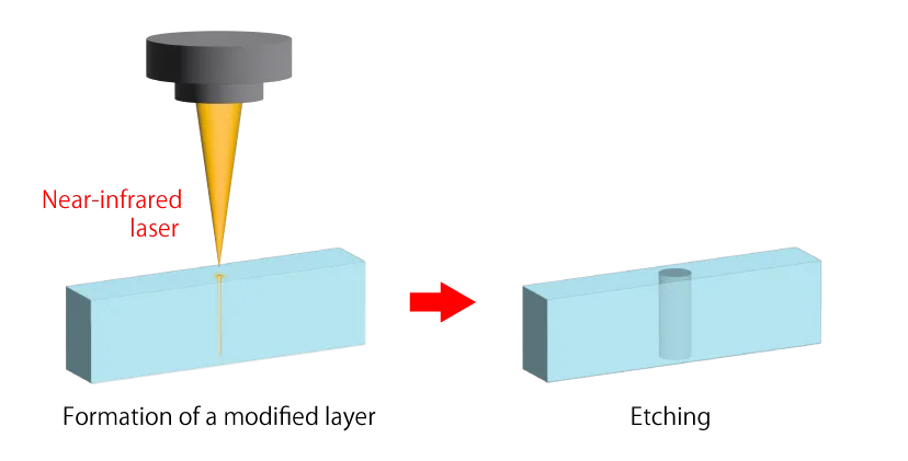
The overall processing time inevitably becomes longer due to the multiple steps involved, such as laser irradiation, cleaning, chemical treatment, and then cleaning again.
-
2: TGV (Through Glass Via): A hole used to electrically connect different layers in a glass substrate. While referred to as a "via" in general substrates, it is called a TGV in glass substrates.
High investment costs
The significant burden of capital investment is also a major challenge. To implement the aforementioned "laser modification and wet etching" method, specialized laser equipment and precise chemical processing systems are required, both of which are extremely expensive. Furthermore, significant costs arise beyond the main equipment itself, such as preparing a safe working environment and installing facilities for properly disposing of used chemicals.
Features of NEG's Glass Substrates
To overcome the challenges of glass substrates, NEG is developing two types of glass substrates:
• GC Core® Substrate
• Glass core substrate
GC Core® Substrate
GC Core® substrates combine the characteristics of glass substrates with the added advantage of easy via processing.
This product utilizes proprietary glass-ceramics developed by NEG, offering the following benefits:
• High-speed, crack-free processing is possible using CO₂ lasers
• Low dielectric constant and low dielectric loss tangent enable high-speed transmission
• Thinner design and improved handling due to high strength
• Specifications can be modified to meet requirements
GC Core® Substrate Lineup
| Type | Low dielectric constant | High-CTE | High mechanical strength | |
|---|---|---|---|---|
| Product Code | GCC-1 | GCC-2 | GCC-3 | |
| Dielectric loss tangent | 2.45 GHz | 0.0013 | 0.0002 | 0.0004 |
| 40 GHz | 0.0016 | 0.0004 | 0.0007 | |
| Dielectric constant | 2.45 GHz | 3.9 | 7.0 | 7.9 |
| 40 GHz | 3.8 | 6.8 | 7.6 | |
| Thermal expansion coefficient (ppm/°C) | 6.1 | 8.9 | 7.4 | |
| Bending strength (MPa) | 150 | 260 | 340 | |
Source: Development of GC Core™ – Glass-Ceramics Core | Nippon Electric Glass (NEG)
Glass Core Substrate
Glass core substrates are core substrates made of glass that offer superior electrical properties and flatness, high rigidity, and enable fine wiring and high-density mounting. The glass substrates produced using NEG's thin glass forming technology, the "overflow method," feature excellent flatness and smoothness, delivering strengths in both quality and cost.
Glass substrates are also being developed by other glass manufacturers, but crack-free via forming has been a challenge for each company. Glass substrates from other companies often require etching for forming via, which also presents issues such as longer processing times.
In contrast, NEG's glass core substrates can also be processed by CO₂ laser processing, enabling high-speed via formation without the use of chemicals. NEG has also successfully developed 515 × 510 mm glass core substrates, contributing to improved production efficiency and reduced environmental impact.
Accelerating Development through Collaboration with Via Mechanics
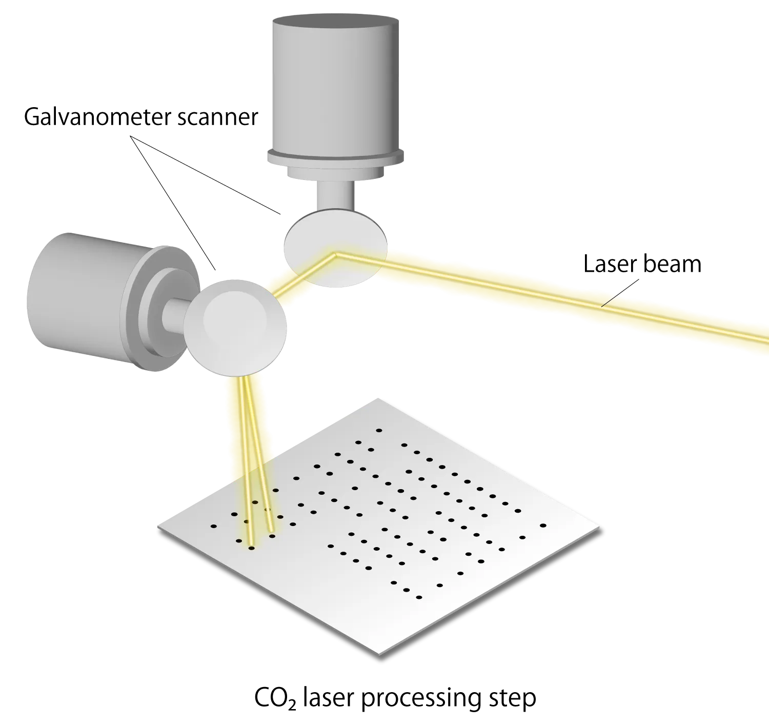
NEG is not only developing its own technology but has also formed a partnership with Via Mechanics, Ltd., a leading manufacturer of substrate drilling equipment, focusing on establishing the processing technology.
In particular, the forming of TGVs, which significantly impacts the performance and yield of glass substrates, requires the integration of material technology and processing technology. Conventional CO₂ laser processing was prone to causing cracks in the glass, posing a major challenge for practical application.
NEG has achieved crack-free CO₂ laser processing by collaborating with Via Mechanics, a company highly regarded in the industry for its laser processing technology.
CO₂ laser processing offers the significant advantage of not requiring specialized chemical treatment equipment, allowing the use of general-purpose laser processing machines. This not only reduces capital investment but also enhances productivity due to fewer process steps.
By combining NEG's cutting-edge glass material technology with Via Mechanics' extensive expertise in CO₂ laser processing, the company aims to achieve the early practical application of glass substrates.
Also Compatible with Laser Modification and Etching Methods
NEG has developed glass substrates compatible with CO₂ laser processing, as well as glass substrates compatible with laser modification and etching methods. Development began in 2020, and the company has been providing glass substrates compatible with laser modification and etching methods since then.
CO₂ laser processing offers the advantage of reduced capital investment since it utilizes standard laser processing equipment. Meanwhile, laser modification and etching methods are also well-suited for forming fine TGVs with small aperture diameters and narrow pitches. Consequently, this technology is advancing in fields demanding high-density packaging, such as semiconductor packages and server CPUs for generative AI.
| TGV processing system | Characteristics | Benefits |
|---|---|---|
| CO₂ laser processing | Direct laser drilling of vias in glass | Fewer steps, high-speed processing, compatible with existing equipment |
| Laser modification and etching | Laser irradiation modifies the glass, enabling selective etching to form vias | Capable of processing TGVs with small diameters and narrow pitches |
NEG provides two types of samples: TGV-processed substrates measuring 515 × 510 mm and unprocessed raw glass sheets.
Not only companies that have already established TGV forming processes using laser modification and etching methods, but also companies that find in-house processing difficult can utilize glass core substrates.
Summary: Strengths of NEG
With the spread of generative AI and the advance of autonomous driving, semiconductor package core substrates are expected to meet increasingly higher performance requirements.
To address these technological advancements, NEG has independently developed GC Core® and glass core substrates compatible with CO₂ laser via processing. Furthermore, the company supports laser modification and etching methods capable of forming small-diameter, narrow-pitch TGVs, offering a comprehensive product lineup to meet diverse needs.
Leveraging extensive expertise gained over many years in developing glass products for a wide range of fields—including displays, electronic components, and optical applications—NEG also offers flexible customization at the material level tailored to specific applications.
Companies interested in glass core substrates, as well as those considering new applications or joint development, are welcome to contact NEG anytime.