Started Development of Glass Core Substrates Compatible with CO2 Laser Processing
The efficiency of the manufacturing process for next-generation semiconductor package substrates will be dramatically improved.
Nippon Electric Glass Co., Ltd. (Head Office: Otsu, Shiga, Japan; President: Akira Kishimoto; “NEG”) has started developing a new glass core substrate that can be drilled using a versatile CO2 laser.
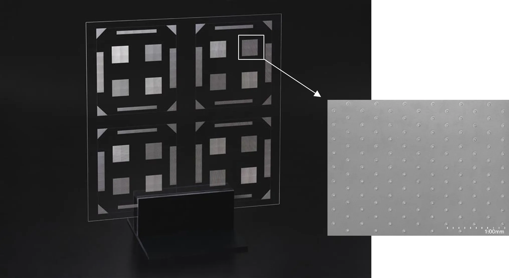
Glass core substrate under development at NEG, which can be drilled with a CO2 laser.
Development background
In recent years, as semiconductors for AI have become more powerful, the chiplet structure* has been increasingly adopted, which in turn has led to larger dice, and an increase in the number of dice, mounted on the core substrate. Along with this trend, there is a growing demand for larger core substrates used to connect semiconductor chips to motherboards.
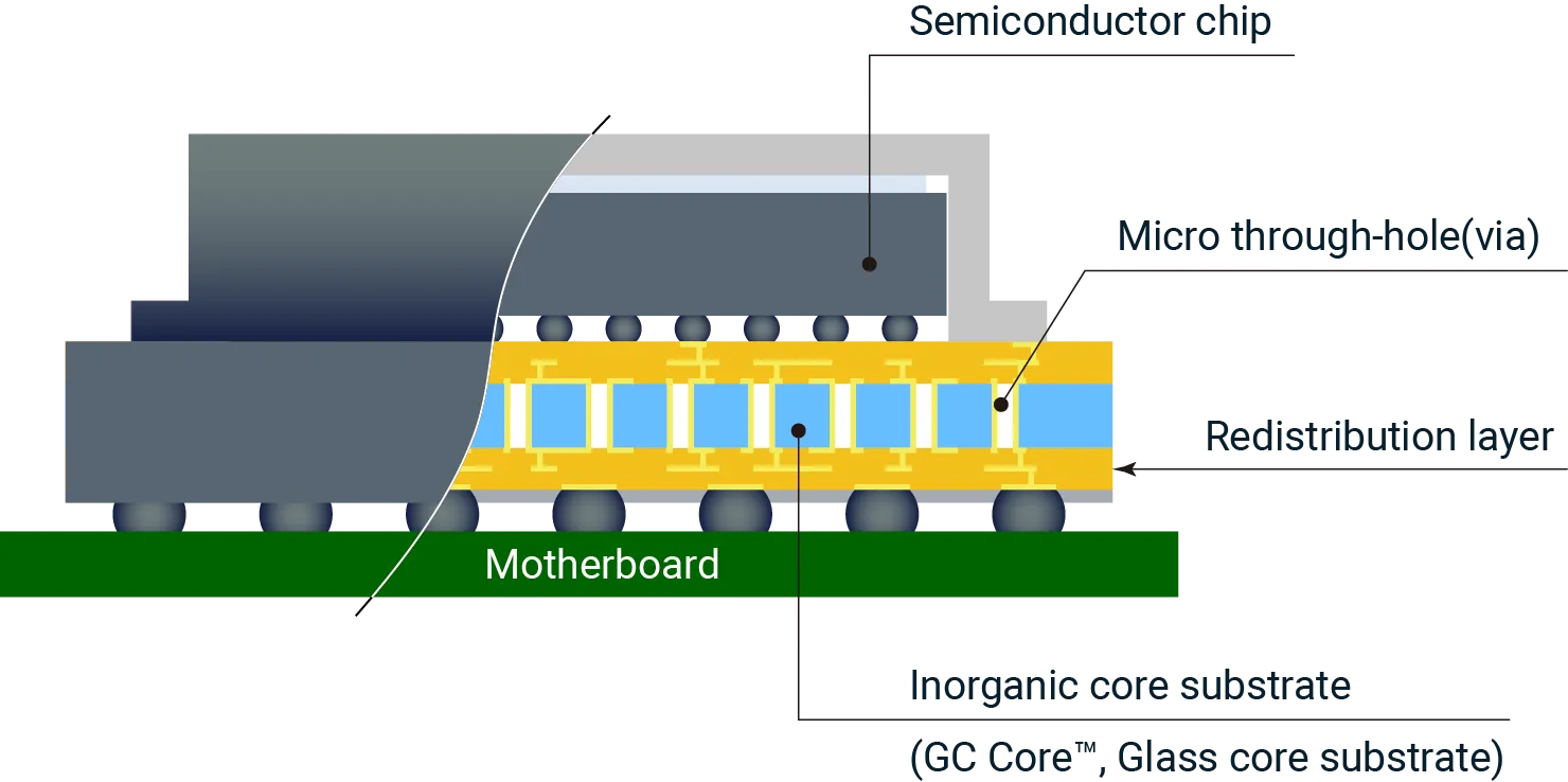
Currently, plastic substrates are the mainstream, but as substrates become larger, issues such as dimensional stability, thermal expansion coefficient, rigidity, and heat dissipation performance arise, making them difficult to support next-generation high-performance, high-density applications. Glass is attracting attention as a material that can solve these issues. However, forming micro through-holes (vias) in a glass core substrate requires a complex process that combines laser modification and acid or alkali etching, posing challenges in terms of technical difficulty, processing time, and capital investment.
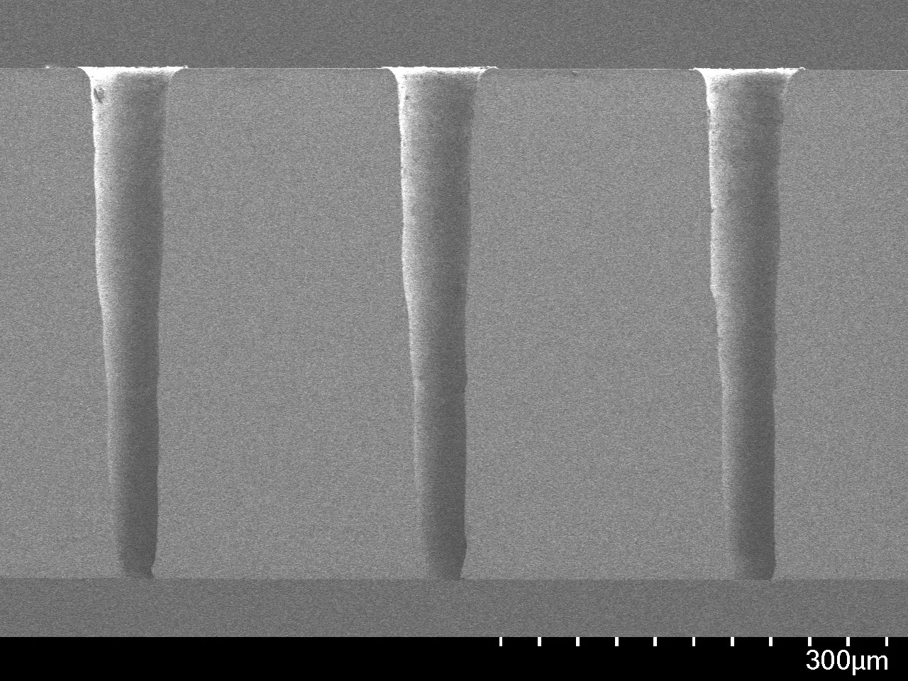
The glass core substrate currently under development will enable the use of a versatile CO2 laser for machining micro-through holes (vias). It will be an innovative technology that overcomes the challenges mentioned above. By optimizing the glass composition and laser processing conditions, NEG has succeeded in drilling crack-free holes in certain hole shapes and continues development with the aim of achieving various hole shapes. Once development is complete, the company plans to add this glass core substrate to its glass core business lineup to meet a wide range of customer needs.
* Chiplet structure
A semiconductor design and manufacturing method that divides functions into multiple small chips (chiplets), rather than the conventional single large semiconductor chip, and connects them using high-performance wiring technology to reduce manufacturing costs and improve performance.
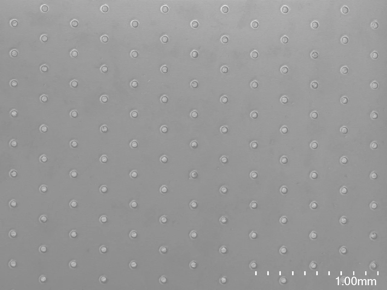
Top section ø75μm, pitch 250μm, substrate thickness 0.4mm
Processed by a laser processing machine of Via Mechanics, Ltd.
Development goals
Increased productivity
- Establish mass production technology using sheet glass forming technology (overflow technology).
- Avoid cracks even during high-speed processing with a CO2 laser.
- Reduce processing time significantly by means of high-speed processing with a CO2 laser.
- Reduce capital investment by using existing manufacturing equipment.
High reliability
- Make the substrate less susceptible to temperature and humidity changes (dimensional stability) and resistant to warping caused by heat or other factors.
- Ensure excellent flatness, smoothness, and rigidity to enable microscopic wiring and high-density mounting.
Future outlook
With GC Core™ (glass-ceramic composite substrate), announced in June 2024, and the glass core substrate currently under development, NEG will expand its line of inorganic core substrates compatible with CO2 laser processing to meet a variety of needs. As the market for semiconductors for AI and data centers expands, demand for inorganic core substrates is expected to increase in the future. As a leading company in key materials that support next-generation semiconductors, NEG will continue to work on continuous technological innovation and product development.
| GC Core™ | Glass core substrate |
|---|---|
|
|
Development progress and future plans
- Study of glass composition and laser processing conditions
- Promoting development with the aim of enlarging the size to 515×510 mm by the end of 2025
- Reliability evaluation currently underway for commercialization
- 300 mm square substrates to be exhibited at SEMICON Japan 2024, scheduled to be held from December 11 to 13, 2024
Exhibition name: SEMICON Japan 2024
Period: Wednesday, December 11 to Friday, December 13, 2024
Venue: Tokyo Big Sight
Booth number: 2135
Exhibition invitation ticket available free of charge at:
Home | SEMICON Japan
Company Profile
Nippon Electric Glass Co., Ltd. is a world-class specialty glass manufacturer headquartered in Otsu City, Shiga Prefecture. Special glass that creates novel functionality is transformed into a variety of products such as sheets, tubes, threads, and powder, and is used in a wide range of fields, including semiconductors, displays, automobiles, electronic devices, medical care, and energy. The special glass developed using the technology and track record that we have honed over our 70-year history is highly regarded in a wide range of fields, from everyday life to cuttingedge industry.
Company name: Nippon Electric Glass Co., Ltd.
Representative: Akira Kishimoto, President
Head office location: 7-1 Seiran 2-chome, Otsu, Shiga 520-8639, Japan
Founded: December 1, 1949
Business details: Manufacture and sale of special glass products and fabrication and sale of glass manufacturing machinery
URL: https://www.neg.co.jp/en
Nippon Electric Glass Co., Ltd. 7-1 Seiran 2-chome, Otsu, Shiga 520-8639, Japan
<Inquiries about our releases>
PR Office, General Affairs Division Phone: +81-77-537-1702 (direct)
<Contact regarding products>
Sales Division, Electronic Products Group Phone: +81-6-6399-2722 (direct)