Development of Large TGV Glass Core Substrates for Laser Modification / Etching and CO₂ Laser Processing
Expanding Our Product Lineup Toward the Full-Scale Development of the Inorganic Core Substrate Business
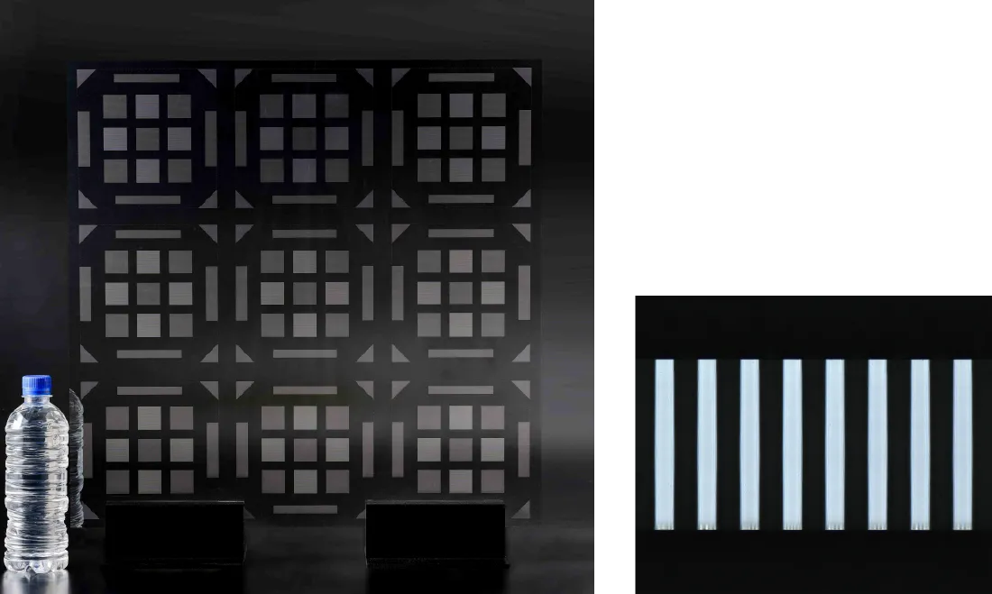
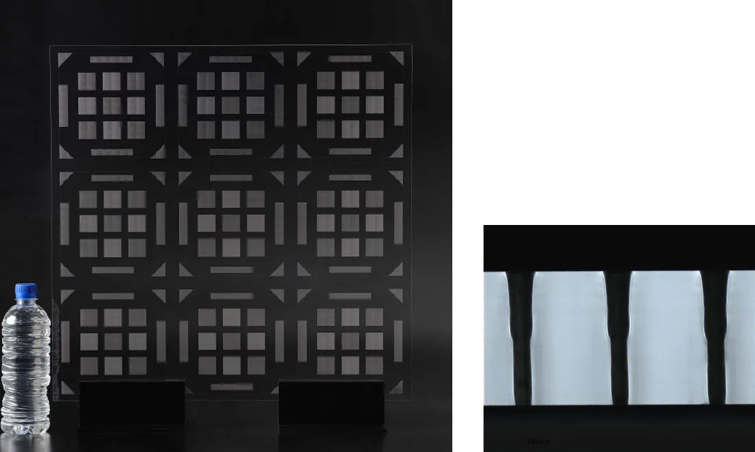
Nippon Electric Glass Co., Ltd. (Head Office: Otsu, Shiga, Japan; President: Akira Kishimoto;) has successfully developed two types of TGV (Through Glass Vias) * 2 glass core substrates for next-generation semiconductor package applications—one compatible with laser modification and etching* 1, and another with CO₂ laser processing—and has begun providing samples of both. The offered products include 515 x 510 mm substrates with TGV processed in-house, as well as unprocessed (TGV-free) mother glass.
With the success of this development, we will further expand our lineup of inorganic core substrates (GC Core™, glass core) and respond to diversifying customer needs in all directions.
* 1 Laser modification and etching: A processing method in which a chemical treatment is performed after forming a via-shaped "modified part" in glass by laser irradiation. Since the reforming part selectively reacts with the chemical solution, fine via processing becomes possible.
* 2 TGV (Through Glass Vias): Ultra-fine through-holes formed in glass substrates for electrical interconnection.
Background of development
Advancements in AI technology and the expansion of data centers are driving demand for increasingly high-performance, high-density semiconductors. The spread of chiplet technology*3 and the trend toward larger package substrates*4 have intensified the need for inorganic core substrates that offer excellent flatness, high insulation, and high rigidity.
As one of the world’s leading specialty glass manufacturers, we have been actively developing advanced materials for inorganic core substrates. We have already received strong interest in our proprietary GC Core™ and glass core substrates designed for CO₂ laser via processing.
Meanwhile, demand has also been growing for TGV processing using laser modification and etching methods. Since 2020, we have been developing glass materials optimized for this method and have provided samples to evaluate. In this latest development, we succeeded in creating a new glass composition ideal for laser modification and etching, and established a sample supply system for large-format substrates (515 x 510 mm) with TGV holes. By offering substrates compatible with both processing methods, we are now better positioned to flexibly and rapidly respond to a broader range of market needs.
*3: Chiplet technology: A semiconductor packaging technology that realizes high performance and flexibility by integrating multiple small chips (chiplets) in one package instead of the conventional single chip configuration.
*4: Package substrate: An intermediate substrate for connecting between a semiconductor chip and an electronic circuit board. It is responsible for electrical connections, heat diffusion, and mechanical support.
Future outlook
We will continue to advance development of inorganic core substrates compatible with CO₂ laser processing—announced in 2024—with the goal of starting mass production by 2028. At the same time, the launch of samples for laser modification and etching will help us gain further customer evaluations and enhance our presence in the inorganic core substrate market.
Exhibition schedule
The inorganic core substrate developed this time will be exhibited at the "Total Solution Exhibition for Electronic Equipment 2025 in JPCA Show 2025" to be held at Tokyo Big Sight from June 4.
Exhibition name: Total Solution Exhibition 2025 (JPCA Show 2025)
Session: June 4 (Wed) - 6 (Fri), 2025
Venue: Tokyo Big Sight
Booth number: 7F-03
Application site for exhibition invitation ticket (free):
Comparison of CO2 laser processing and laser modification / etching
|
TGV processing system |
Characteristics |
Benefits |
|
CO2 laser processing |
Direct laser drilling of vias in glass |
Fewer steps, high-speed processing, compatible with PCB*5 laser processing machine |
|
Laser modification and etching |
Laser irradiation modifies the glass, enabling selective etching to form vias |
Capable of processing TGVs with small diameters and narrow pitches Etching surface is not easily damaged |
* 5 PCB: Printed circuit boards
Inorganic core substrate product page